T1 Circuit Diagram
Wiring t1 diagrams evo What is e1 line T1 e1 line
Equivalent circuit during [t0, t1]. | Download Scientific Diagram
Equivalent circuit during [t0, t1]. Loopback t1 plug make cable diagram wiring testing line dsu csu rj45 cat both jack wire spiceworks off inches cut Cisco collaboration: t1 and e1 circuits (for ccna ccnp & ccie
T1 circuit circuitlab description
T1 wiring pinout2014 tech study guide: schematics and components (part 1) Circuit t0 equivalentT1 basic system circuit mile wires copper repeaters four every so.
T1 wiring diagram / diagram in pictures database rj45 t1 wiring diagramWiring ds1 T1 e1 cisco circuits collaboration ccnp ccna ccie candidates benisnousBasic circuit diagram-t1+t2 pv surge protection device flp-pvxxxg-s.

Components t1 schematics tech study guide part kb6nu electrical radio ham diagram schematic
T1 crossover cable pinout diagramT0 simplified T1 pinout wiringT1 circuits.
How to make a t1 loopback plug for testing both line and csu/dsuCybertanz blog: a brief about the t1 T1 telecom lines t3 network communicationT1 basic circuits.

Circuitlab capacitors
T1 wiring diagramSchematic depiction of the switching circuit. t1 and t2 mark the power T1 wiring diagramDepiction switching t2 transistors.
T1 circuit 1 capacitorsPinout diagram cable t1 db25 parallel port crossover wiring pinouts ground connector connectors connections svg file supply serial computer many Simplified circuit during [t0, t1].Surge pv flp spd.
![Equivalent circuit during [t0, t1]. | Download Scientific Diagram](https://i2.wp.com/www.researchgate.net/profile/Yanxue_Yu/publication/282896464/figure/fig11/AS:668707474915334@1536443694407/Equivalent-circuit-during-t0-t1.ppm)
Pots, public switched telephone network & internet telecom
T1 wiring guide .
.
![Simplified circuit during [t0, t1]. | Download Scientific Diagram](https://i2.wp.com/www.researchgate.net/profile/Yanxue_Yu/publication/282896464/figure/download/fig3/AS:354311872761859@1461485941705/Simplified-circuit-during-t0-t1.png)

Basic Circuit Diagram-T1+T2 PV Surge Protection Device FLP-PVxxxG-S

POTS, Public Switched Telephone Network & Internet Telecom

How to make a T1 Loopback plug for testing both Line and CSU/DSU

Schematic depiction of the switching circuit. T1 and T2 mark the power
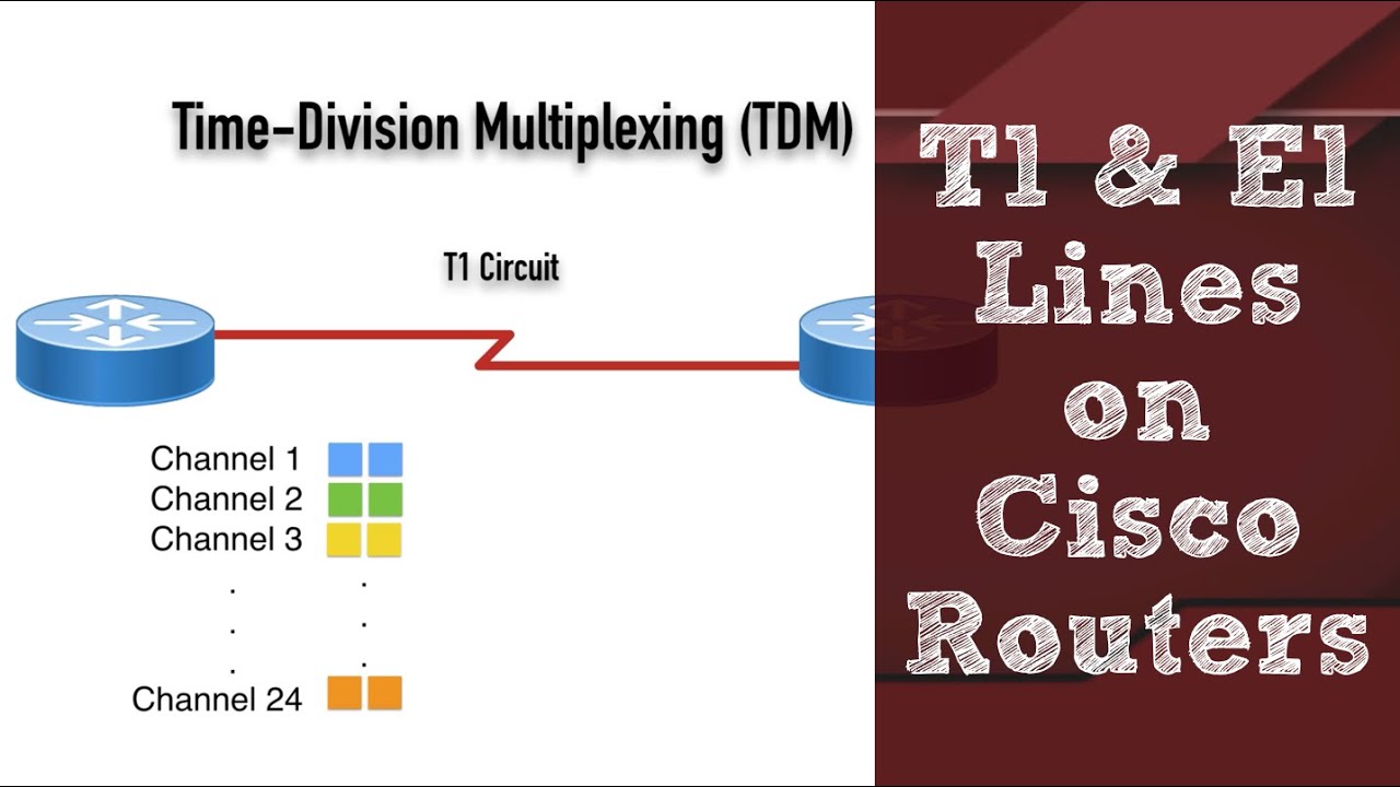
Cisco Collaboration: T1 and E1 Circuits (for CCNA CCNP & CCIE

T1 Crossover Cable Pinout Diagram - Wiring Diagram Pictures
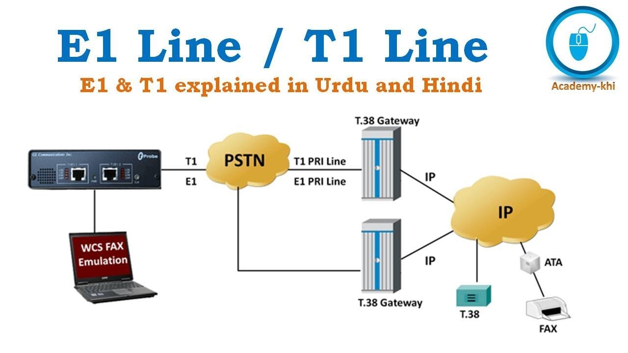
What is E1 line | What is T1 line | E1 and T1 Explained in Urdu and

2014 Tech study guide: schematics and components (part 1)